I like tinkering with schematic based logic design, but I can easily find myself distracted away from the technical problem at hand by trying to make my schematic nice and neat. Using code instead of a schematic will let me abstract away this problem while also providing means of making my designs more scalable and easier to understand.
In this post I'll export a schematic based design from Digital to run on a real FPGA and I'll also look at how custom blocks in Verilog can be added into a schematic design in Digital.

Digital Goes IRL
So far in this series all of the circuit tinkery has been virtual, but the HDL exporting features in Digital will let us bring these designs to life.
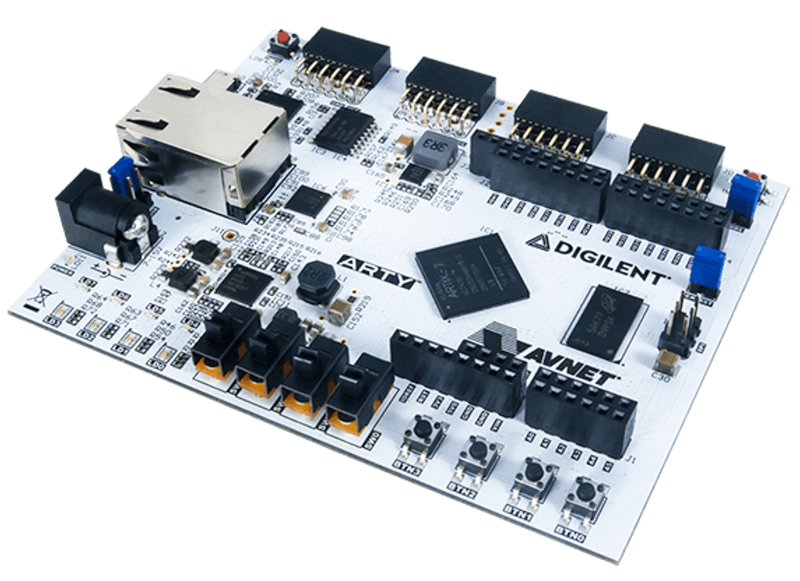
I'll first come up with a rough plan. The Arty-A7 board I will use has enough lights, buttons and switches for me to play around with, so that is not a big concern.
The schematic has one big issue though: the telnet block is actually powered my magic (or simulator software) so it can't be exported to HDL. That's not a dealbreaker for today's goal though, I'll just... simulate the emulated hardware with actual hardware, obviously!
Since the telnet block is going away, so does the communication protocol from before and so I'll simplify the schematic a bit before getting deeper into this.
That cleans up a good bit of clutter. The register now has floating inputs so I'll need to route some new signals to it. This is also a good time to replace the switches and LEDs in the design as those physical devices are also not part of the HDL model of the digital world. Everything will get simplified down to inputs an outputs at the top level.
I'm not sure if Clk needs to be changed, I guess we'll find out when I try to export it!
So Clk wasn't a problem, but all of my other pins being unlabeled was. After slapping some names on them, Digital is ready to export it to Verilog for me.
Let's see what it generated...
/*
 * Generated by Digital. Don't modify this file!
 * Any changes will be lost if this file is regenerated.
 */

module DIG_Register_BUS #(
    parameter Bits = 1
)
(
    input C,
    input en,
    input [(Bits - 1):0]D,
    output [(Bits - 1):0]Q
);

    reg [(Bits - 1):0] state = 'h0;

    assign Q = state;

    always @ (posedge C) begin
        if (en)
            state <= D;
   end
endmodule

module top (
  input Clk,
  input r1,
  input r2,
  input t,
  input s1,
  input s2,
  output l1,
  output l2
);
  wire [1:0] s0;
  wire [1:0] s3;
  assign s0[0] = r1;
  assign s0[1] = r2;
  DIG_Register_BUS #(
    .Bits(2)
  )
  DIG_Register_BUS_i0 (
    .D( s0 ),
    .C( Clk ),
    .en( t ),
    .Q( s3 )
  );
  assign l1 = (s1 ^ s3[0]);
  assign l2 = (s2 ^ s3[1]);
endmodule
It's interesting to see what kind of HDL it generated for me. There's a module digital made to represent it's version of a register and the top module which is my design. I named the file top.v so that the module would be named top and that is conventionally the name for the top level module in an FPGA project.
Some FPGA Wizardry
One of my side projects, which will hopefully be receiving some more love in the near future, is a tool to aide in this kind of digital tinkery called Wiz. My aim for this tool is to make playing with FPGAs a lot easier and more fun, especially for curious software developers.
As of this writing the tool is very young and in rough shape, but it's made for this exact type of exploratory usage so here we go!
I'll start by creating a new folder, and within that folder I'll make a wiz.toml file, this is a manifest file used by Wiz that tells it how I want to build and program my logic design project.
package_name = 'irl'
builder = 'vivado'
programmer = 'vivado'
target_part = 'xc7a35ticsg324-1L'
target_device = 'xc7a35t_0'
source_files = ['top.v']
bitstream_path = 'irl.bit'

[pins]
This file format is very likely to change, but the important parts are that vivado is what I'll be using for building and programming the device and it also specifies some details about my target Artix-A35T FPGA part/device.
I'll also need to add more detail to the [pins] section to map out the FPGA pins to the inputs and outputs of my top module. This is mostly going to be a matter of referring to the board reference material and selecting from that.

In this case, I'll use the Arty's LD7 and LD6 LEDs as LED1 (l1) and LED2 (l2), which are mapped to pins T10 and T9 respectively. For the physical switch inputs (s1 and s2), I'll use the left two dip switches (SW3 and SW2) and for the register inputs (r1 and r2) I'll use the right two (SW1 and SW0). For t, my trigger input to save the new register state, I'll use the BTN0 button. That just leaves Clk, which I'll hook up to the 100mhz clock on FPGA pin E3.
[pins]
Clk = 'E3'
r1 = 'C11'
r2 = 'A8'
t = 'D9'
s1 = 'A10'
s2 = 'C10'
l1 = 'T10'
l2 = 'T9'
Picking and mapping the pins can be a little tedious, but professional FPGA tools often make it much more work than this!
Next I'll build the project with wiz build
It takes a good bit to get through all its steps, but at the end I have my bitfile ready to flash. I'll plug in my Arty board and load it up with wiz program.
Huzzah, my design is now implemented and working in real hardware!
The design itself isn't very interesting, but I'm pretty happy with the flow my Wiz tool is starting to enable.
Returning to Schematics
Now what I'll do is a little bit of the opposite direction, just to prove that these tools can be mixed and matched. I'll make a new schematic and include a new Verilog block that includes the design. This is the exported Verilog from earlier, but this time imported into Digital as a module.
Everything needs to match up, including the one Clk signal I capitalized for no reason and the top module name for the block. I now have a pretty decent grip on a flow for how to mix and match HDL and schematics for logic design. That'll be all for this post!