So I'm working on designing my own homebrew 6502-based microcomputer. I have a lot of ideas for features I'd like, but before I make too many crazy decisions I'd like to solidify my understanding of the processor I'm building the whole system around. To this end, I am grabbing my Arty-A7, a W65C02S mounted on a breadboard and a bag of jumper cables to wire them together.
Planning Phase
I chose to use my Arty-A7 FPGA board because it has a ton of I/O pins, it can easily meet my performance requirements and because I just plain love tinkering with FPGAs.
This will take a smidge of organization to get started. I began by taking an inventory of the various pin functions on the W65C02S package.
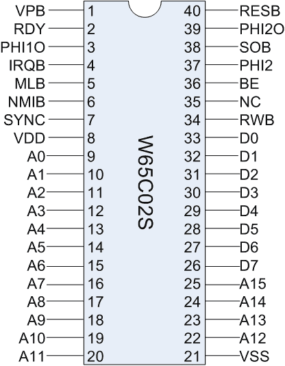
Generally speaking, there are 16 pins for the address bus, 8 pins for the data bus, 13 control pins, 2 power pins and 1 no-connect. This means I’ll need to wire 37 IO pins + 2 power pins to my FPGA board. With that in mind I’ve decided to use a mix of the PMOD interfaces on my Arty board as well as the Arduino-shield pins next to them. Each PMOD has 8 IO pins so I’ll use 1 PMOD for the data bus and 2 for the address bus, with the control pins on adjacent shield header. I’ll pull power from one of the PMODs as well.
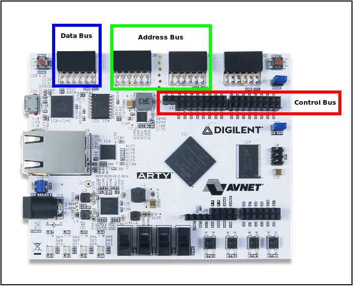
With my rough plan in place, I took some notes on how my 6502 pins will map to the specific pins. I planned for which PMOD pin each bit of the address and data buses will go, along with associating each control pin to a numbered shield pin. Now for the fun part!
Wired Up
Now that the rough planning is complete, I carefully use the wire jumpers to connect everything as planned. I wired one pin at a time roughly starting from the top of the 6502 and working down, it’s a bit of a mess but it does the job.
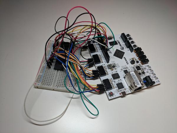
Now that the plumbing is in place, the real fun begins. I start by opening up Vivado and begin getting these pins mapped into a design. I’ll create a new top.sv file to kick off the design.
`timescale 1ns / 1ps

module top (
  // Arty stuff
  input  logic clk_100mhz,
  input  logic reset,

// 6502 stuff
  input  logic [15:0] address,
  inout  logic [7:0] data,
  input  logic vpb,
  input  logic phi1o,
  input  logic phi2o,
  input  logic rwb,
  input  logic mlb,
  input  logic sync,
  output logic resb,
  output logic sob,
  output logic phi2,
  output logic be,
  output logic irqb,
  output logic nmib,
  output logic rdy
);

endmodule
The next step is to tediously map the various pins I planned out to the pins on the pins I’ve defined in my top module. The PMOD pins are easily found in the reference wiki for the board, but I didn’t see the IO shield pins on the primary documentation page, so I referred to the provided schematic files for that information. With all that pin mapping information, I added the pins properties into a constraints file.

At this point, everything looks to be ready for tinkering. As an initial experiment to validate that it is working, I’ll use IP block to manually probe and interact with these pins. Though, just before I generate that, I’ll add a few more lines to my
top.sv to support bi-directional use of the data bus. For the 6502, when the rwb pin is high, the CPU is reading from the data bus, so I’ll use that as the trigger to put my write_data on that data bus during those times.
logic [7:0] write_data;
assign data = (rwb) ? write_data : 'bZ,
    sob = 1,
    be = 1,
    irqb = 1,
    nmib = 1,
    rdy = 1;
Once I am running on real hardware, I’ll be stepping through the reset logic for the 6502. So for this project irqb, be, nmib, rdy and sob can all stay at 1 for now, as I won’t be using them.
Now seems like the time to start building the VIO block. I’ll add ports for the various inputs and outputs, including the register I just added for bi-directional communication on the data bus.
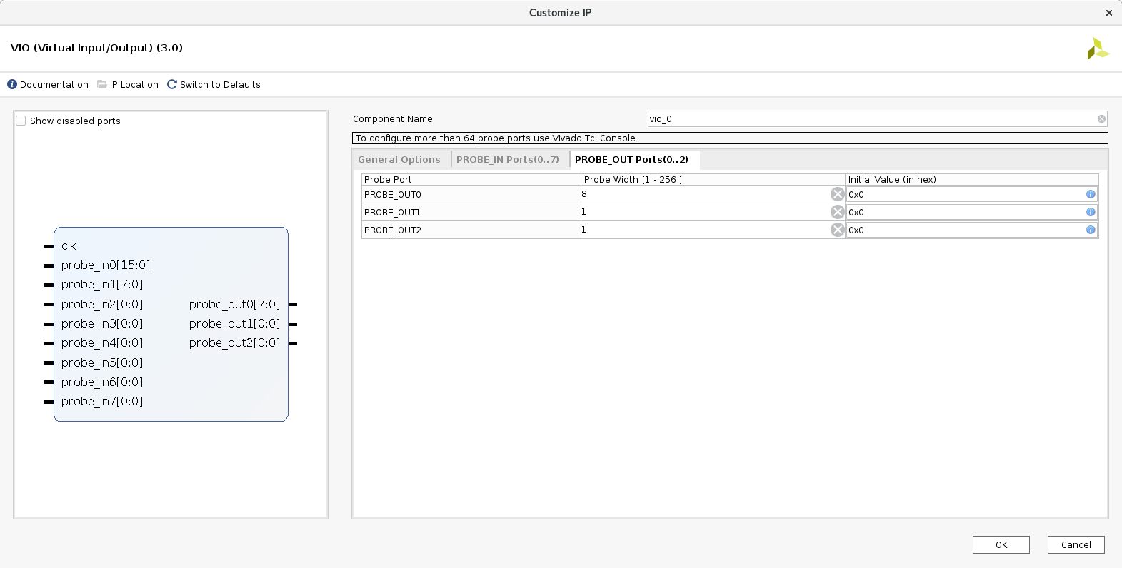
I’ll let Vivado synthesize the core, and I’ll add it to the top module.
vio_0 debug_core (
    .clk(clk_100mhz),         // input wire clk
    .probe_in0(address),      // input wire [15 : 0] probe_in0
    .probe_in1(data),         // input wire [7 : 0] probe_in1
    .probe_in2(vpb),          // input wire [0 : 0] probe_in2
    .probe_in3(phi1o),        // input wire [0 : 0] probe_in3
    .probe_in4(phi2o),        // input wire [0 : 0] probe_in4
    .probe_in5(rwb),          // input wire [0 : 0] probe_in5
    .probe_in6(mlb),          // input wire [0 : 0] probe_in6
    .probe_in7(sync),         // input wire [0 : 0] probe_in7
    .probe_out0(write_data),  // output wire [7 : 0] probe_out0
    .probe_out1(resb),        // output wire [0 : 0] probe_out1
    .probe_out2(phi2)         // output wire [0 : 0] probe_out2
)
Now it is time for the moment of truth!
Playing with a Running CPU
With all that in place, it’s time to build everything and start playing around. After running synthesis, implementation and generating a bitfile, I can flash my new design and debug core to the Arty board and pull up the VIO interface that shows me the current state of things.
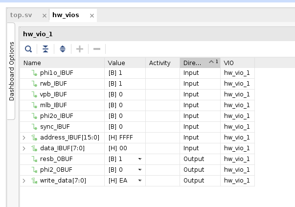
At this point a bit more knowledge on the how the 6502 operates is necessary. The phi2 signal is the input clock for the CPU. The core of this 6502 is fully static, so this clock can be stopped at anytime and the state within the CPU preserved. This allows me to interact and step the clock manually through VIO, even though my manual input will be extremely slow for interacting with hardware.
Since the clock looks good, I’m going to perform a reset of the 6502. Near the end of the reset cycle I’m expecting the address bus to read for the reset vector, a pointer to where the CPU should begin execution after reset. For the timing requirements on getting a reset to work properly, the documentation from WDC states specifically what to do:
3.11
Reset (RESB)
The Reset (RESB) input is used to initialize the microprocessor and start program execution. The
RESB signal must be held low for at least two clock cycles after VDD reaches operating voltage.

…

When a positive edge is detected, there will be a reset sequence lasting seven clock cycles. The
program counter is loaded with the reset vector from locations FFFC (low byte) and FFFD (high
byte). This is the start location for program control. RESB should be held high after reset for
normal operation.
So I’ll hold reset low for at least 2 cycles, then set it back to high. I’ll continue to manually cycle the clock until I see CPU begin to fetch the RESET vector. As that vector is read, I will manually give it the address 0xDEAD to begin execution at. Then, to keep it running I’ll give it the opcode 0xEA (NOP) so it continues to read empty instructions over the bus. It’s worth noting that the 6502 does most things in alignment to the falling edge of the phi2 clock.
The 6502 has been reset and is running the instructions it’s reading from the FPGA! In the future I’ll extend this design to better simulate an imaginary system. That’ll be my stopping place for today, hope you enjoyed!